PCB Design That Breaks the Mold
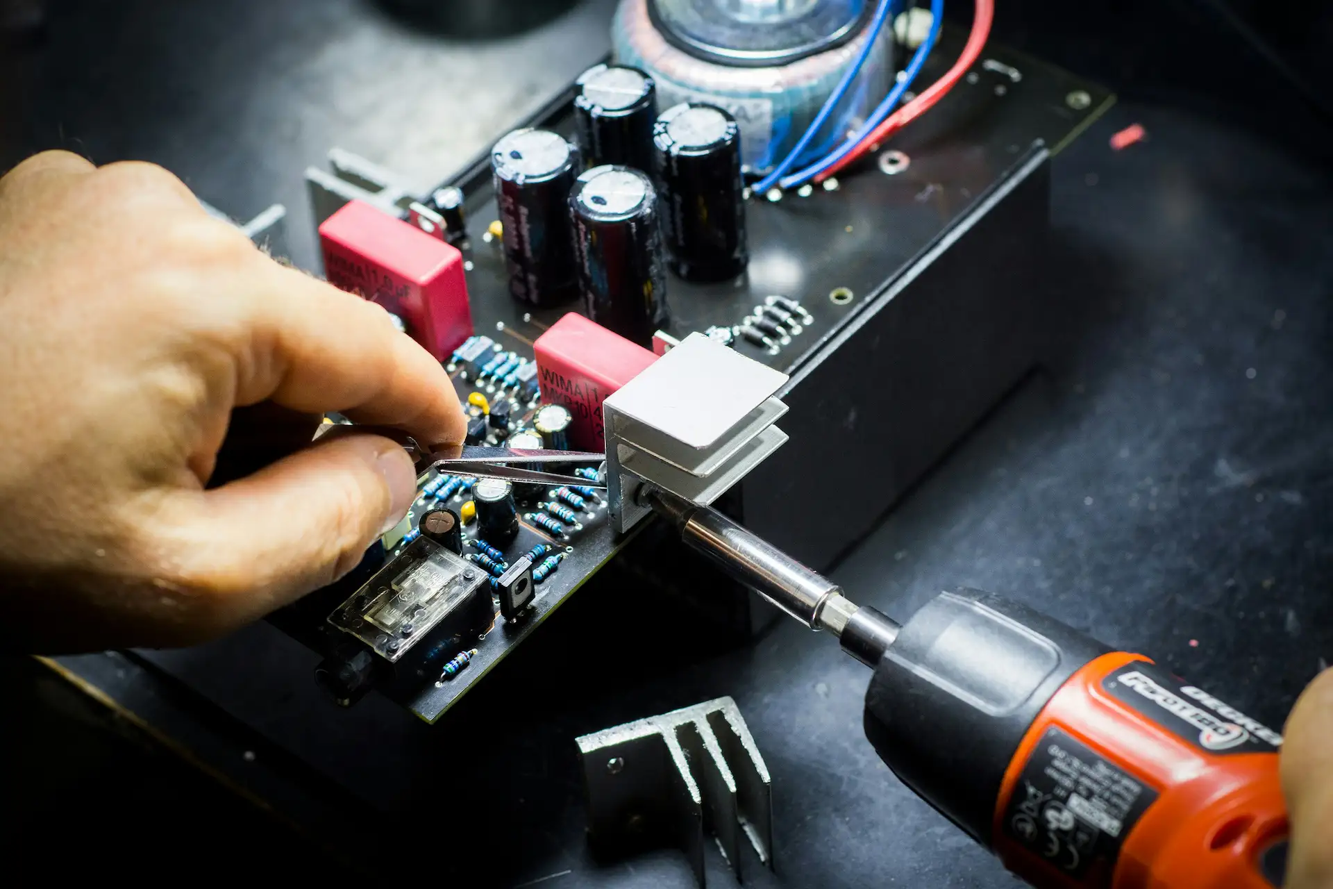
At CustomPowerLabs, we don’t believe in one-size-fits-all solutions—we engineer one-size-fits-YOU designs. PCB design isn’t just about placing components on a board; it’s about crafting a tailored solution that integrates seamlessly into your project, no matter how unconventional the requirements. Whether you need fully custom sizing, complex topologic structures, or double-stacked PCBs to maximise functionality in ultra-compact spaces, we deliver designs that push the boundaries of what’s possible.
We thrive on solving challenges that other manufacturers might shy away from. Need a PCB precisely 12.7 mm wide to fit within a bespoke enclosure? Consider it done. Looking for a board that twists, bends, or integrates into an intricate 3D assembly? We’re already mapping out the layout. Our commitment to customisation ensures that no dimension, shape, or configuration is off-limits—if you can conceptualise it, we can engineer it.
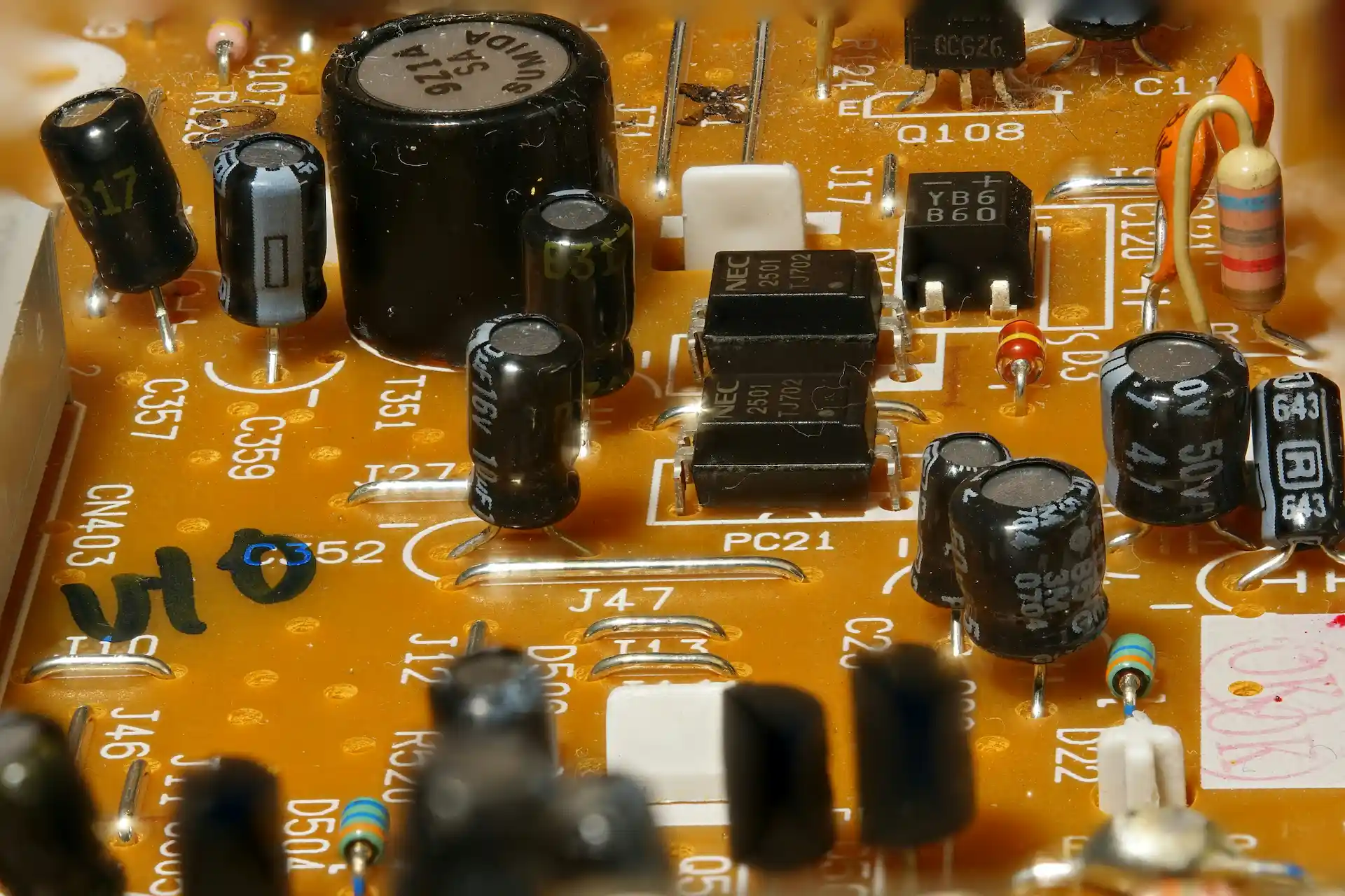
Beyond just form factor, we optimise every aspect of our designs for efficiency, durability, and performance. Whether it’s a high-density PCB for a cutting-edge wearable, a thermally managed layout for industrial automation, or a multi-layered powerhouse for aerospace applications, we tailor every detail to your specific needs. At CustomPowerLabs, customisation isn’t just an option—it’s our specialty. We don’t settle for ordinary, and neither should you.
Our Superpower: Unmatched Flexibility
At CustomPowerLabs, flexibility isn’t just a feature—it’s the foundation of everything we do. Standard PCB templates and restrictive design limitations don’t belong in our vocabulary. Instead, we engineer solutions that stretch, shrink, bend, and stack to fit your exact requirements. Whether your project calls for unconventional dimensions, intricate layouts, or multi-layered stack-ups, we’ll tailor a PCB design that integrates flawlessly into your system. No minimum orders, no “that’s not possible”—just precision engineering shaped entirely around your needs.
We specialise in creating PCBs that adapt to the most challenging constraints. Need a custom-sized board that fits within millimetre-tight tolerances? We’ll get it right the first time. Working with curved, flexible, or multi-plane enclosures? We’ll design a rigid-flex hybrid that conforms effortlessly to your form factor. Our double-stacking technology allows us to layer PCBs vertically, maximising functionality while maintaining a compact footprint—perfect for applications where space is at an absolute premium.
Beyond size and structure, we refine every detail to optimise electrical performance, thermal management, and mechanical integrity. Whether you need a board with intricate trace routing to minimise signal loss or a high-density component layout for mission-critical applications, our expertise ensures you get a PCB that doesn’t just fit—it excels. At CustomPowerLabs, customisation isn’t an afterthought—it’s our speciality. Whatever your vision, we’ll turn it into reality with engineering precision and uncompromising flexibility.
Features That Redefine What’s Possible
Fully Custom Sizing: Precision Without Limits
When it comes to PCB design, standard sizes and shapes often force engineers to compromise. At CustomPowerLabs, we eliminate those restrictions by offering fully custom sizing, ensuring that your board conforms precisely to your project’s requirements. Whether you need a 5 cm × 2 cm ultra-thin rectangle for a sleek wearable, a 17 mm circular board for a compact sensor, or an irregularly shaped design to fit a unique enclosure, we make it happen with millimetre-perfect precision.
Our custom-cut PCBs don’t just fit—they integrate seamlessly into your hardware, reducing unnecessary bulk and maximising efficiency. No arbitrary constraints, no design compromises—just pure adaptability tailored to your project’s needs. Whether you’re working on a prototype or scaling to mass production, we deliver boards that align with your vision down to the last detail.
Topologic Structures: Engineering That Pushes Boundaries
PCBs don’t have to be flat, boring slabs. At CustomPowerLabs, we specialise in advanced topologic structures that redefine conventional circuit board design. Our expertise allows us to create rigid-flex hybrids, intricate layouts with multi-dimensional routing, and bendable, foldable PCBs that adapt to complex enclosures and unconventional form factors.
Whether you need a PCB that wraps around corners, folds into tight enclosures, or integrates seamlessly into 3D assemblies, we’ll engineer it with the precision needed for flawless operation. Every trace is routed with optimal efficiency, ensuring signal integrity, EMI mitigation, and mechanical durability. Our designs don’t just function—they become a structural and electrical advantage within your system.
Double-Stacking PCBs: More Power, Less Space
When compact designs demand maximum functionality, our double-stacking PCB technology delivers. By vertically layering multiple PCBs, we enable designs that double processing power, expand I/O capabilities, and enhance signal integrity without increasing footprint size. This technique is a game-changer for IoT devices, aerospace applications, high-density medical electronics, and next-generation computing modules.
Our double-stacked PCBs are engineered with thermal dissipation, EMI shielding, and structural integrity in mind. We ensure that stacked layers remain electrically efficient, mechanically robust, and production-ready. If your design is pushing the limits of space constraints, this technique allows you to pack more functionality into less volume—without sacrificing performance or reliability.
Where Our Flexibility Shines
At CustomPowerLabs, we don’t just design PCBs—we engineer solutions that push the limits of size, shape, and performance. Whether it’s a compact wearable, a life-saving medical device, or a mission-critical aerospace system, our custom PCBs adapt to the most demanding environments with precision and reliability. Here’s where our ultra-flexible designs make a difference:
- Wearables & Smart Devices: The next generation of compact electronics demands ultra-thin, uniquely shaped PCBs. Whether it’s a curved smartwatch PCB, a sensor-laden fitness tracker, or an ultra-slim hearing aid, our custom sizing and double-stacked designs ensure maximum functionality in minimal space.
- Medical Technology: From implantable devices that require biocompatible, ultra-miniaturised PCBs to advanced diagnostic tools with precision power delivery, our tailored solutions meet the stringent demands of healthcare innovation. Our PCBs are optimised for low noise, ultra-reliability, and minimal power consumption, ensuring safe and effective operation.
- Aerospace & Defence: Space constraints, extreme conditions, and absolute reliability—our PCBs thrive where failure is not an option. Lightweight, thermally-optimised, and topologically engineered, our stacked and flex-rigid designs are used in satellites, avionics systems, and military-grade electronics that demand cutting-edge durability and performance.
- IoT & Embedded Systems: Smart technology is shrinking, but its complexity is growing. Our PCBs power everything from smart home automation to industrial IoT sensors, ensuring seamless connectivity, energy efficiency, and long-term reliability. With our multi-layer stacking and compact routing solutions, we deliver powerful, space-efficient designs that keep your devices running at peak performance.
- Custom & Experimental Devices: Have a concept that doesn’t fit traditional PCB manufacturing constraints? Whether it’s an experimental research prototype, a next-gen robotics component, or a product that defies conventional design rules, our custom topology, exotic material integration, and high-density PCB layouts bring even the most ambitious ideas to life.
With CustomPowerLabs, your project isn’t bound by traditional PCB limitations. No matter how unique or challenging your requirements, we have the expertise to engineer a perfect-fit solution that exceeds expectations.
FAQs About Our Custom PCB Design
Can you really design PCBs in any size or shape?
Absolutely! Whether you need a microscopic board for a medical implant, a circular PCB for a wearable, or a completely irregular shape for a custom enclosure, we can make it happen with precision engineering.
How does double-stacking PCBs help with space constraints?
Think of it like a high-rise building—more functionality without expanding the footprint.
Benefits of double-stacking:
- Optimised signal routing: Reduces electromagnetic interference and improves performance.
- Enhanced power efficiency: Better heat dissipation and reduced energy loss.
- Compact integration: Ideal for space-constrained applications like wearables and IoT devices.
Are custom PCBs more expensive than off-the-shelf solutions?
Not necessarily! A tailored PCB can actually lower overall system costs by:
- Eliminating unnecessary components.
- Optimising layout for efficient material use.
- Reducing assembly complexity and manufacturing costs.
What makes your topologic structures different from standard PCB layouts?
Unlike traditional flat PCB designs, our topologic structures allow for:
- Bending and folding: Ideal for compact and wearable electronics.
- Multi-plane integration: Improves mechanical fit and signal integrity.
- Flex-rigid hybrid designs: Combines the best of both worlds for dynamic applications.
What industries benefit most from your custom PCB designs?
We design for a broad range of industries, including:
- Wearables: Ultra-thin, flexible, and lightweight PCBs.
- Medical devices: Precision-engineered boards for implants and diagnostic tools.
- Aerospace: High-reliability and radiation-resistant designs.
- IoT: Miniaturised, power-efficient PCBs for smart devices.
- Industrial automation: Rugged designs for high-performance applications.
- Experimental electronics: Prototyping unique circuit solutions.
Can you help with thermal management and high-current applications?
Yes! We use advanced thermal dissipation techniques to ensure reliable operation.
Key features:
- High-current trace routing for power-dense applications.
- Multi-layer copper strategies for improved heat dissipation.
- Thermal vias and heat sinks to maintain safe operating temperatures.
How do I get started with a custom PCB design?
It’s easy—just reach out with your project specs!
Our process:
- Consultation: Discuss your design requirements and constraints.
- Engineering & Prototyping: We refine your design for performance and manufacturability.
- Production: Whether you need low-volume or high-volume manufacturing, we tailor the process to your needs.
Have more questions? Contact us today, and let’s build a PCB solution that perfectly fits your project!